Nanomesh
Boron Nitride Nanomesh as a Scaffold for Functional Surfaces, Nanocatalysts and Molecular Electronics

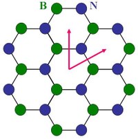
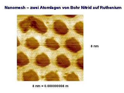
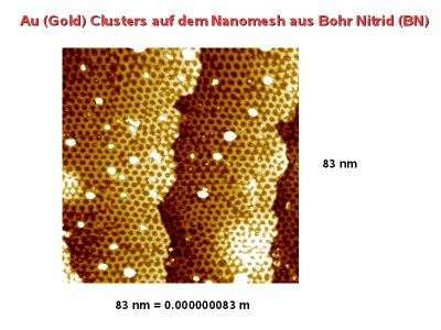
When the BN is deposited on Ru(0001), by exposing it to B3N3H6 at 1050K, a BN nanomesh is formed developing a highly regular hexagonal array of circular holes ~2nm in diameter separated by the distance of ~3nm. A comprehensive multitechnique analysis shows that the BN film actually consists of two BN planes. However, the exact and complete atomic model, meaning a full set of atomic coordinates (metal, boron and nitrogen atoms) is still lacking. Below are the STM images, showing the n-BN/Ru(0001) and various gold clusters on the nanomesh.


Due to extremely high chemical and thermal stability of BN, the nanomesh looks like a perfect scaffold for patterning molecules or metal clusters with a wide variety of novel chemical, biological, magnetic or electronic properties. One can imagine producing ordered arrays of molecules with appropriate size, or depositing metal on the nanomesh - forming ordered clsuters inside the holes. This can lead to a wide variety of applications in nanochemistry (nanocatalysis), nanophysics (nanoelectronics, nanomagnetism), biotechnology, etc. On the other hand, the selforganization process leading to nanomesh creation is a matter of great fundamental interest. This process is unique in terms that roughly 400 atoms take part in the concerted creation of a single unit cell!
Goals of the Nanomesh project:
1. Uncover the atomic structure of the nanomesh which means to determine exactly all atomic coordinates, including those of the substrate atoms; Here a full understanding can be achieved only by a selfconsistent combination of STM, SPA-LEED and X-ray crystallography techniques.
2. Try to create the nanomesh with cheaper and easier to handle substrates and precursors, which may open the way for mass production and commercial applications. Things under considerations: metal films on insulator and semiconductor wafers as substrates, 3-chlorborazine is a precursor with a very easy handling.
3. Use the nanomesh as a natural inorganic and carbon-free scaffold to pattern nanosized metal clusters. This will lead us to realm of nanocatalysis: investigation of catalytic properties of nanosized metal clusters (e.g. Pt, Pd, Rh, etc.). Another interesting problem is to compare the catalytic properties of a pure Ru(0001) substrate (exposed with its entire surface to the reactants) and the one covered with nanomesh (that is exposed to reactants only through thin 3 nm holes).
4. Try to commercialize any of the findings, through creation of spin-off startups.
Nanomesh is EU specific targeted research project NMP4-CT-2004-013817.
Official web-site of the project: www.nanomesh.ch
