February 2010The image shows a cross section of about 2 µm photoresist and 200 nm gold deposited on a silicon substrate. This is an inspection of a photolithography process for micro structured gold electrodes via scanning electron microscopy. The resist areas covered by a mask during light exposure were removed in a solvent. Depending on the process parameters the shown resist undercut profile can be prepared, which provides a non-conform gold coating (i. e. the resist walls stay uncoated). During the wet chemical lift-off process the resist starts to dissolve at these areas.The small inlet shows a top view of the gold electrodes after lift-off. Picure submitted from P. Hartmannhttps://www.uni-giessen.de/en/faculties/f08/departments/physchem/janek/gallerypotm/gallery-of-pictures-from-2010/february-2010/viewhttps://www.uni-giessen.de/@@site-logo/logo.png
Document Actions
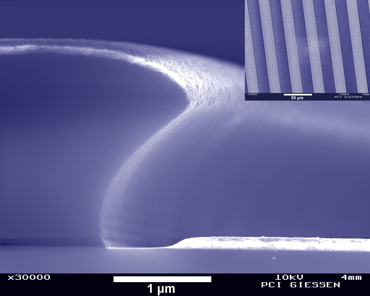
February 2010
The image shows a cross section of about 2 µm photoresist and 200 nm gold deposited on a silicon substrate. This is an inspection of a photolithography process for micro structured gold electrodes via scanning electron microscopy. The resist areas covered by a mask during light exposure were removed in a solvent. Depending on the process parameters the shown resist undercut profile can be prepared, which provides a non-conform gold coating (i. e. the resist walls stay uncoated). During the wet chemical lift-off process the resist starts to dissolve at these areas.The small inlet shows a top view of the gold electrodes after lift-off. Picure submitted from P. Hartmann
