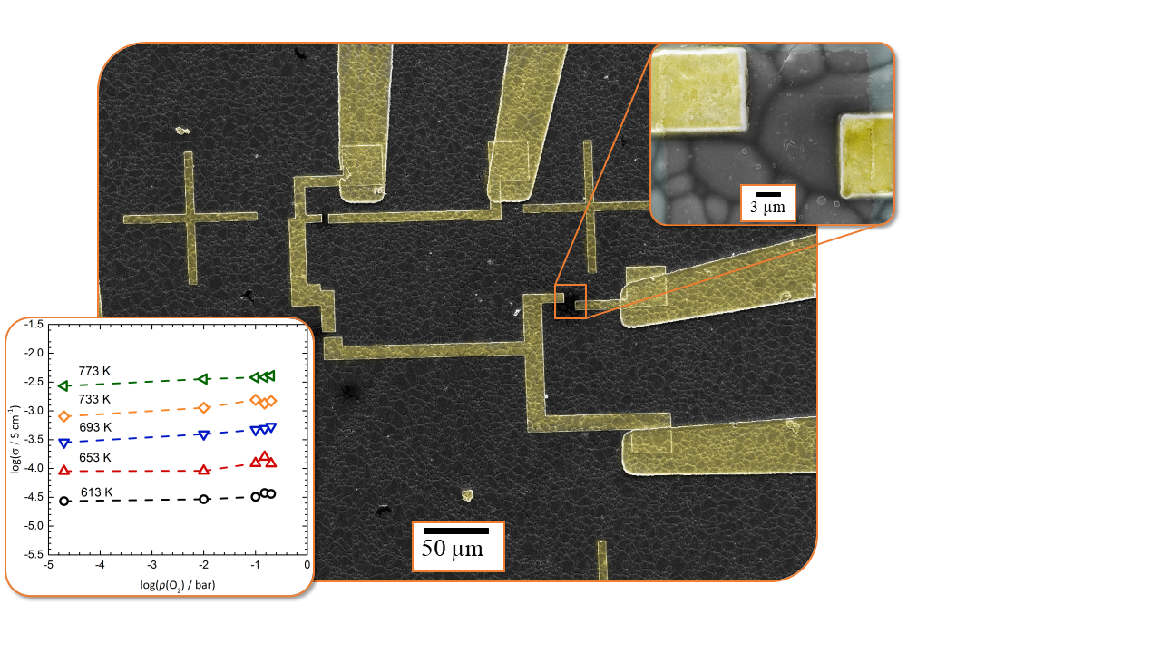
December 2018To resolve the conductivity of both individual grains and grain boundaries within a ceria (CeO2) thin-film, gold microelectrodes were deposited in such a way that only a minimal area of the grains would be exposed to the gold, thereby preventing unwanted conduction pathways throughout the thin-film. To accomplish this, an insulating layer of alumina (Al2O3) was deposited on top of the thin-film in order to cover everything except the desired contact areas on the grains. For this and for the preparation of the electrodes, several iterations of photo and electron beam lithography were employed. At first, the fine structures at the grains were transferred, followed by the deposition of the contact pads on the edge of the thin-film, which were needed to connect the sample to the measurement setup.With these electrodes, it was possible to perform impedance spectroscopy on both individual grains and grain boundaries at temperatures up to 773 K, while varying the oxygen partial pressure in order to gain insight into the differences in defect chemistry arising from space charge layer effects. (Picture submitted by Julian Zahnow.)https://www.uni-giessen.de/en/faculties/f08/departments/physchem/janek/gallerypotm/pom2018/BdM1218.png/viewhttps://www.uni-giessen.de/@@site-logo/logo.png
Document Actions
December 2018
To resolve the conductivity of both individual grains and grain boundaries within a ceria (CeO2) thin-film, gold microelectrodes were deposited in such a way that only a minimal area of the grains would be exposed to the gold, thereby preventing unwanted conduction pathways throughout the thin-film. To accomplish this, an insulating layer of alumina (Al2O3) was deposited on top of the thin-film in order to cover everything except the desired contact areas on the grains. For this and for the preparation of the electrodes, several iterations of photo and electron beam lithography were employed. At first, the fine structures at the grains were transferred, followed by the deposition of the contact pads on the edge of the thin-film, which were needed to connect the sample to the measurement setup.With these electrodes, it was possible to perform impedance spectroscopy on both individual grains and grain boundaries at temperatures up to 773 K, while varying the oxygen partial pressure in order to gain insight into the differences in defect chemistry arising from space charge layer effects. (Picture submitted by Julian Zahnow.)
